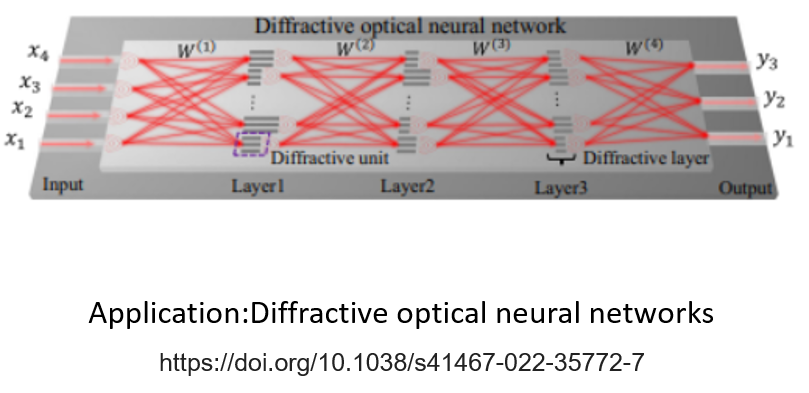
Due to the rapid development of artificial intelligence-related application technologies, the demand for network bandwidth and transmission bit rate is increasing day by day. In the past, integrated circuits were the main focus of development. However, electricity has shortcomings such as slow speed, high loss, and signal interference. Replacing integrated circuits with optical integrated circuits has become a trend in the development of high-speed computing technology. Similar to integrated circuits, silicon photonics chips use various combinations of optical waveguide components to enable optical systems to exhibit different functions and characteristics. Its application includes high-speed computing, optical communication, detection technology, etc. are expected to significantly replace existing optical component configurations in the near future. Visera’s goal is to become a foundry including design and manufacturing services. The most efficient way is to develop optical waveguide devices process design kit (PDK) with excellent performance. Customers are allowed to choose the component for circuit design in product development. The PDK must be well developed and include a wide range of specifications to choose from. The current development progress has completed the basic optical waveguide design part. It is expected to complete the R&D prototype production in 2025 and establish a complete measurement platform to test the performance of optical waveguide components. In 2026, it is expected to mature the PDK to provide customers with a full range of designs and OEM services.


