1.1.1 Ownership
VisEra Technologies Company Ltd. (hereinafter referred to as "VisEra" or "the Company") was established on December 1, 2003 as a joint venture of Taiwan Semiconductor Manufacturing Company Limited (hereinafter referred to as "TSMC") and a foreign partner. TSMC purchased the partner's shares in 2016 and VisEra is now a subsidiary of TSMC. VisEra aims to be one of the best and largest professional semiconductor optical component and manufacturing service provider in the world. In June 2022, the Company's shares were listed on the Taiwan Stock Exchange.
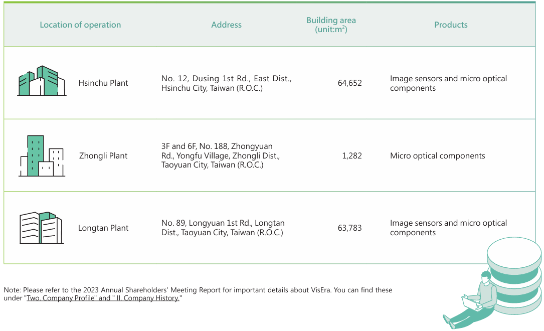
• Head office address: No. 12, Dusing 1st Rd., East Dist., Hsinchu City, Taiwan (R.O.C.)
•Stock Code: 6789
•Industry: Listed semiconductor industry; the Sustainability Accounting Standards Board (SASB) industry classification system categorizes it as "Semiconductors"
• Capital: NT$3.166 billion (as of December 31, 2023)
• Number of employees: 1,387
• Annual revenue of the year: NT$7.237 billion
1.1.2 Description of Main Products
VisEra focuses on the OEM of image sensors and wafer-level optical components and mainly engages in the image sensor production and services for back-end processes, including color filter manufacturing, wafer-level test services, and on-chip multi-film manufacturing. It is one of the few professional OEM manufacturers in the world that provides color filter process, micro lens process, and multi-film process and integrates technologies for use in product manufacturing.
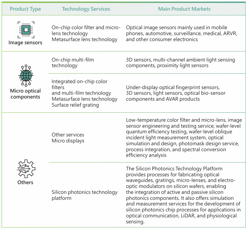
Image sensor product foundry business
In recent years, customer products, whether in automotive, imaging sensors or smartphone imaging sensors, have been a trend towards 12” development in the manufacturing process technology of color filter, and continuously pursuing improvements in sensing efficiency. Our company proposed exclusive optical structure design for color filter film in 2023, which has been mass-produced to enhance the quantum efficiency (QE) of small pixel spectra. Currently, we are also working on the development of the second-generation product, which is estimated to introduce to customers for mass production in the second half of 2024. Besides, we developed Nano Light pillars, nanometer microstructures for CIS, which have been successfully verified on 0.8um. Samples sent to major customers have also received positive feedback, aiming to improve QE (quantum efficiency) and sensitivity on mobile phones and automotive sensors. Expected to complete development by 2024.
Wafer-level optical components foundry business
• Continuously developing new-generation high-quality coating process technology for 3D sensing component products. This product has been verified and adopted by world-renowned manufacturers, and has been utilized in successive generations of products. It is still being shipped steadily currently.
The newly developed multiple-channel light sensing coating technology has been verified and put into mass production in 2021 for use in various optical thin film products. In addition, many clients have adopted this technology. In terms of distance and 3D sensing technology, VisEra provides integrated technology for micro-lenses and narrowband filter multi-layer coating processes, simultaneously enhancing optical efficiency and achieving module thinning. Mass production goals have been reached.
• Surface relief grating technology
AR/VR is regarded as the potential product of the next generation, and our developed SRG surface relief grating technology is considered to be one of the key factors in whether AR/VR can become a consumer-grade product. It enables the fabrication of optical routing structures within limited substrate area and thickness conditions.
•Metasurface Technology
In the future, in addition to continuing refining existing color filter film and optical thin film manufacturing processes, the focus of new technological development will be meta-surface technology and biosensing chips for the next phase of market layout.
Our Company will continue to develop various optical manufacturing processes to enhance integration efficiency, providing customers with excellent wafer-level semiconductor process optical component OEM services.
1.1.3 Main Markets
On-chip color filter and micro-lens market
The main products in the on-chip color filter and micro-lens market are image sensors used for smart phones, automobiles, and surveillance cameras. The Company' s image sensor technology mainly provides the sensors required in the mobile device, automobile, and surveillance camera markets. Although facing headwinds in the mobile phone market and CIS inventory adjustments in 2023, overall shipments slightly declined. However, the shipment of high-end image sensors increased to 64 million pixels and 50 million pixels, and mainstream market sensors continued to rise to 8 million pixels, indicating that the overall market is still moving towards higher pixel densities. Based on the market research data on VisEra's client terminals shipment, it is estimated that VisEra is still maintaining a comparable market share as in the past. The Company will still maintain a leading position in the fabless foundry market in terms of high-resolution and small pixel (<0.7μm) technology. In the future, we will continue to cooperate with the top customers in the market, and continue to expand our presence in the mobile phone with 50 million pixels and automotive markets.
Integrated on-chip multi-film market
The Company's integrated on-chip multi-film technology consists mainly of 3D optical sensing components, ToF sensor technology and ambient light sensor. 3D optical sensing components and ToF sensor technology are held by certain manufacturers. While the ambient light sensor, due to active development in standardized product markets in recent years, is estimated to capture over fifty percent market share in the ambient light sensor market.